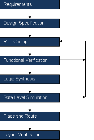
Step I: Requirement specification is prepared to
o define the function to be achieved,
o have technical inputs from experts,
o contain things like cost of the product, time to market etc.
Step II: Design specification is written to describe the overall architecture, functionality and various interfaces of the circuit. Block diagram description is added here.
Step III: Behavioral description is created from specifications and written with RTL. The RTL description can be implemented in any HDL like Verilog, VHDL, System Verilog etc.
Step IV: Now EDA (Electronic Development Automation) tools come into picture. Functional verification tests the RTL against the design specification. Semantic checks and synthesizability of RTL is also done here.
Examples of verification tools:
Linting tool: Spyglass (for semantic checks)
Verification tool: Modelsim, NCSim, VCS, Incisive IFV, Magellan etc.
Step V: Logic synthesis converts the RTL code to gate level netlist. A gate level netlist is a description of the design in terms of gates, memories, wires etc.
Examples of synthesis tools: Precision, Synplicity, Design Compiler etc.
Step VI: Gate level simulation is required to test netlist against the RTL/design-specification. Here Formal Verification, Static Timing Analysis (STA), Scan-Tracing, Equivalence checking is also done.
Step VII: Synthesized netlist along with constraints file is passed to PNR tool for back end activities like Floor planning, Placement, Routing etc. And Layout is created.
Step VIII: Layout verification involves STA, Design Rule Checks, Functional Verification etc.